Components and Parts Idea/Ad Exchange, free for members. > West
> Manufacturing
> Xa single board computer developer kit
Xa single board computer developer kit
HI-TECH Software XA Single Board Computer
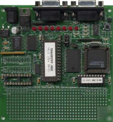
The XA Single Board Computer from HI-TECH Software is designed to allow a potential user of the XA microcontroller to evaluate the chip, or implement a first prototype without the time and expense of producing a custom PCB.
Pin Connections and Memory Map
*Acrobat files require the Acrobat Reader from Adobe.
The XA Single Board Computer from HI-TECH Software is designed to allow a potential user of the XA microcontroller to evaluate the chip, or implement a first prototype without the time and expense of producing a custom PCB. Included on the board are:
* XA-G30 microcontroller operating at 30MHz
* 128K bytes of low-power static RAM
* 32-128K bytes of EPROM (in standard 28 or 32 pin DIP socket)
* Dual serial ports with RS232 drivers on DB9 connectors
* 8 LEDs for debugging purposes
* Two external interrupt inputs and two timer inputs
* 8 bits each of parallel input and output
* Data bus with address decoding for I/O expansion.
* Remote debugger in EPROM with matching PC software for easy downloading and debugging.
* Socket for the Maxim MAX186 8-channel 12-bit A/D converter
* Requires unregulated 7-9V DC supply (plug-pack or similar)
* Breadboard area for prototyping
The XA Single Board Computer is approximately 4 inches (10cm) square. On one side are two DB9 connectors for serial interfacing. Each connector is a female DB9 wired as a DCE, and thus requiring only a straight cable to plug into a standard PC 9 pin serial connector (supplied). Adjacent to the serial connectors is a coaxial DC connector, with a 2.1mm centre pin. This is wired to a bridge rectifier, so the DC power supply polarity does not have to be specific.
Behind the serial connectors are 8 LEDs, for debugging purposes. The lower third of the board is a prototyping area with an unconnected hole matrix, and ground and power holes. Provided on the board are two 20 way connector pads for connecting parallel input and output, and access to the data bus. The XA EX0 and EX1 pins (labelled as INT0 and INT1 respectively on the board), and T0 and T1 are accessible via pads at the top of the prototyping area.
The board requires 7 to 9V DC, supplied to the coaxial DC connector. Included is a single phase diode bridge to allow either polarity from the power supply. Current drain is approximately 300mA. A 7805 regulator is provided on board, next to the power connector. This is not provided with a heatsink and should not require one unless the input voltage is higher than 9V or the current drain is significantly increased by additional components. If you do fit a heatsink, it must be insulated from the board, as there are tracks on top of the board underneath the regulator. A fibre washer between the heatsink and board will suffice.
To set the board up, it may be useful to mount it on insulating standoffs with the four holes at the corners of the board. Plug the supplied EPROM into the ROM socket. Note that the socket is a 32 pin socket, but the supplied EPROM has 28 pins (27256). It should be plugged into the socket bottom-aligned, i.e. there should be four spare pins adjacent to the LEDs.
Plug the supplied straight cable (i.e. not a null-modem cable) with a DB9 male connector into the DB9 connector J2 (on the opposite side of the board from the power connector). The other end of this cable should plug into COM1 or COM2 of your PC.
Connect a plug-pack or other DC power supply, providing 7-9V at 300mA, into the DC power connector.
Turn the plug-pack on. The LEDs will sweep up and down once, and then leave at least one LED illuminated. If you do not see this, check the power supply.
Once the board is connected to the serial port of your PC, you can then download and debug programs with the software provide. The software agent is called Lucifer. It is a remote source-level debugger, the usage for this software is outlined in the manual.
1.6 Compiling your own programs
To compile your own programs, use HPDXA as supplied with the HI-TECH compiler for the XA. You must select large model from the Options/Memory model and chip type dialog, and you should set the following memory addresses:
This will allow you to access nearly 32K bytes of data memory (Lucifer uses 7F00-7FFF) and 96K bytes of code memory. Note that the data memory at 0 is also mapped as code memory at 80000h, which is why the ROM address should be set at 88000h, to avoid conflict with RAM used as data memory.
Most of the XA I/O pins are used for address and data lines on the board. The remaining I/O pins are either connected to the serial ports, or brought out to labelled pads at the top right of the breadboard area. These pins allow access to the external interrupts and timer inputs.
Additional I/O is provided with 74HC373 latches, and a 74HC244 input buffer. The LEDs are driven by a latch at address E0000h (note that two of the LED bits are shared with the ADC). Writing to address E8000h will latch data into another 74HC373, while reading the same address will gate data in through a 74HC244. These input and output lines are available on J1 along with power and ground. There is no handshaking on these ports.
For further I/O expansion, J5 provides access to the data bus, 5 address lines, a select signal and read and write strobes. You can use these to address up to 32 bytes of data at address F0000h.